TS2068 Serial Port Documentation
Version 1.0
(For informational purposes only.)
*** Due to a miscalculation of the distance required between the edge connector and the top of the TS2068 case the adapter cannot be plugged in with the case fully and properly seated ***
*** Also, due to an incorrectly labeled foot print a DB9 male connector was laid out instead of the a DB9 Female. This requires the that DB9 be mounted on the etch side of the board ***
*** I got caught, twice, by the order of the data lines on the expansion connector. ***
*** There was also the small issue that M1 and IORQ occur simultaneously for interrupt acknowledge, and there are a lot of those, requiring that the address decoding be reconfigured using a 7421 instead of a 7411 ***
*** I got turned around on the MAX232 thinking that Vs+ and Vs- were for a single capacitor instead of each to ground resulting in the MAX232 not developing the correct plus and minus voltages ***
As of 07-16-2023 all required corrections have been made to board #1. A corrections sheet is being developed and will be published when validated.
If you still, in spite of the above, would like to have one
of these boards contact me at ![]() for $5.25 each plus whatever postage is
required. My preferred payment method is Zell.
for $5.25 each plus whatever postage is
required. My preferred payment method is Zell.
Additional information on the driver code required can be found under the Flash Dissembler topic.
Parts
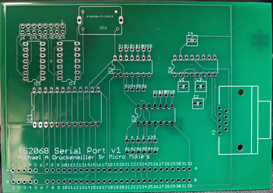
IC1 – MC68B50 [“B” Required if using 1.8432 MHz Crystal for QG1]
IC2 – 74LS04 5 spared gates with vias for patching
IC3 – 74LS11 1 Spared gate with vias for patching
IC4 – 74LS92
IC5 – 74LS93
IC6 – MAX232
QG1 – 1.8432 MHz Full Can Crystal Oscillator Jameco PN 27879
X2- DB-9 (RS-232) Must be mounted on the back side to clear TS2068. * See Page 5
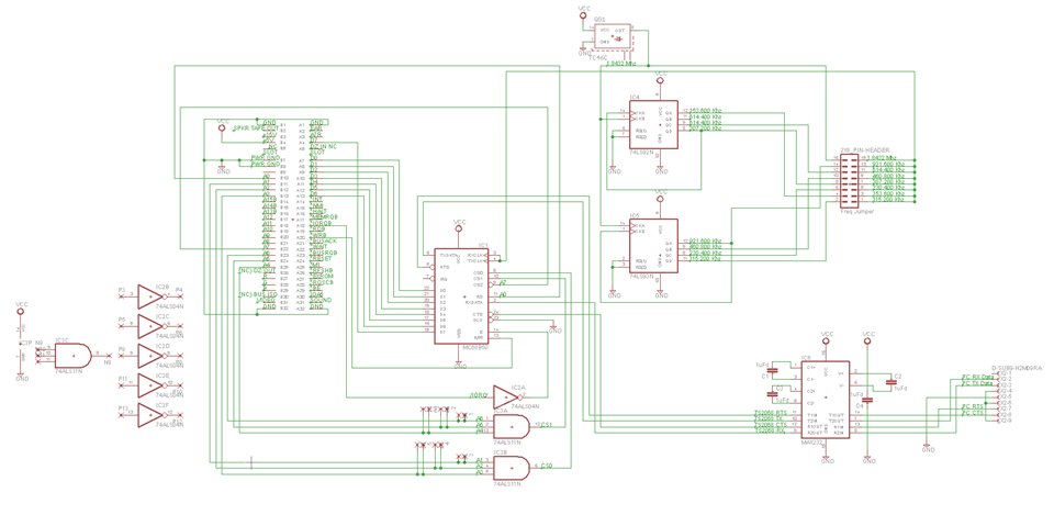
Hardware decoding is for I/O 126 & 127
A7 – LOW – to CS2!
A6, A5, A4 – HIGH to IC3A to CS1
A3, A2, A1 – HIGH to IC3B to CS0
A0 – to RS
01111110 – 126 – Control Register
01111111 – 127 – Data Register
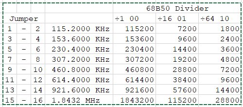 The 2 x 8 Pin
Header provides the ability to jumper one of the divided clock frequencies for
the baud rate.
C1-4 Are 1mFd If Polarized Capacitors are used the following should be noted.
Positive Pins
1 C1 – Right
2 C2 – Left
4 C3 – Left
16 C4 – Right
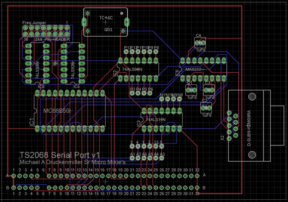
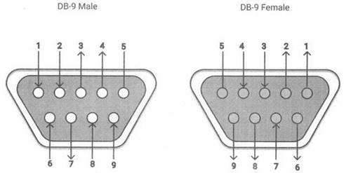
When viewed from component side:
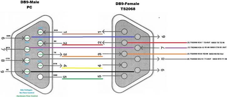
If DB9-Female is mounted use DB9-Male pinning as guide
If DB9- Male is mounted, I suspect you need to use DB9-Female Pinning
When Viewed from the component side the Pinning is correct.
